Our group focuses on the epitaxial growth of multifunctional oxide thin-films and heterostructures using oxide molecular beam epitaxy. We measure their electrical transport behavior, and develop prototypical devices. We also collaborate extensively with other groups for additional characterization of our heterostructures (e.g., X-ray diffraction, STEM, HAXPES, etc.). Some areas of current interest are discussed below.
Electrically coupling multifunctional oxides to semiconductors
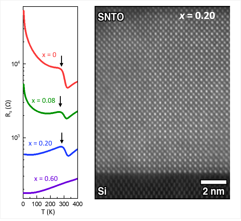
Heterojunctions between semiconductors and multifunctional oxides potentially enable material functionalities that cannot be achieved in either material alone, by virtue of their mixed covalent and ionic natures. We are interested in elucidating pathways by which the charge, spin, polarization, and optical degrees of freedom between oxides and semiconductors can be coupled to realize functional behavior.
Sample publications:
“Charge Transfer and Built-in Electric Fields Between a Crystalline Oxide and Silicon,” Z. H. Lim, N. F. Quackenbush, A. Penn, M. Chrysler, M. Bowden, Z. Zhu, J. M. Ablett, T. -L. Lee, J. M. LeBeau, J. C. Woicik, S. A. Chambers and J. H. Ngai, Phys. Rev. Lett. 123, 026805 (2019).
“Surface termination control of charge transfer across a semiconductor-crystalline oxide interface,” M. Chrysler J. Gabel, T.-L. Lee, Z. Zhu, T. C. Kaspar, P. V. Sushko, S. A. Chambers, and J. H. Ngai, Phys. Rev. Mater. 7, 084604 (2023).
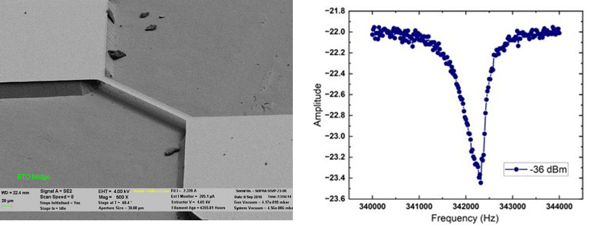
Oxide-based microelectromechanical systems
We have a growing effort in exploring multifunctional oxide materials in microelectromechanical systems (MEMS). As the electronic properties of oxides are strongly coupled to their physical structure, mechanically altering physical structure via stress opens a pathway to tune electronic response in active devices. Yet more intriguing, the common perovskite structure enables oxides that differ in chemical composition to be monolithically integrated into a common epitaxial stack. We seek to elucidate behavior that emerges in such heterostructures through active mechanical perturbation.
Sample publication:
“Suspended single-crystalline oxide structures on silicon through wet-etch techniques: effects of oxygen vacancies and dislocations on etch rates,” Z. H. Lim, M. Chrysler, A. Kumar, J. P. Mauthe, D. P. Kumah, C. Richardson, J. M. LeBeau and J. H. Ngai, J. Vac. Sci. Technol. A 38, 013406 (2020)
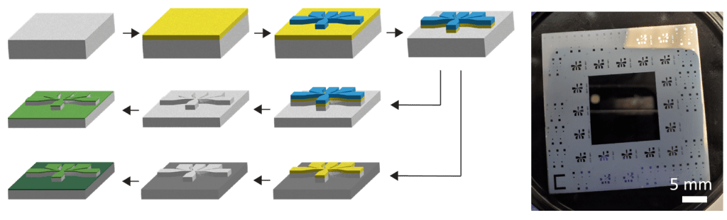
Integration of oxide devices on Si
Oxides exhibit a variety of properties that can potentially be exploited in next-generation device applications, such as ferroelectricity, ferromagnetism, high-temperature superconductivity, and resistive switching. While integration of epitaxial oxides on Si has been achieved, realizing functional devices on Si remains a work in progress. We are interested in developing post-deposition techniques to pattern and create oxide-based devices on silicon. We are also working on deposition-last approaches, in which the Si wafer is first patterned prior to film growth.
Sample publication:
“Deposition-last Lithographically Defined Epitaxial Complex Oxide Devices on Si(100),” M. Chrysler, J. C. Jiang, G. Lorkowski, E. I. Meletis, and J. H. Ngai, J. Vac. Sci. Technol. A 40, 052701 (2022).